Double patterning requires new critical etches capable of sub-1.5 nm CD uniformity, pattern shrink and in situ full-stack etching.
Raghu Balasubramanian, Andy Romano and Marshall Benham, Lam Research Corp., Fremont, Calif. -- Semiconductor International, 2/1/2008
A multitude of double patterning (DP) or multiple patterning methods are being investigated, virtually all of which require additional etch process steps. While there are substantial differences in the DP schemes used between device types, a few common critical etch requirements have emerged that relate to DP implementation. These include the need for <1.5 nm 3s CD uniformity from all etch sources for the 3× nm technology node, the ability to perform in situ shrink and etch for holes and spaces, and the drive for cost efficiency to balance the increasing number of etch steps.
Overlay will be one of the technical challenges for DP in production. Etch CD uniformity is confounded with overlay in DP. Therefore, the etch process must minimally contribute to CD non-uniformity to keep the overall overlay budget manageable. It is expected that tight CD uniformities will be required, pushing etch control to a few atomic layers and making etch for DP a critical application. Achieving overall CD uniformity targets requires understanding and controlling the factors that impact the etch environment. In addition, the ability to monitor plasma with advanced diagnostic sensors and process complex information to tighten run-to-run control will be essential for delivering repeatable results.
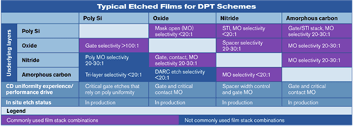
One important consideration in engineering a successful DP scheme is choosing films with appropriate selectivities. The Table shows film types suitable for DP and the relative etch selectivities. The DP materials are based on film stacks used for CD-critical applications, such as mask open, spacer and gate. Thus, from the etch point of view, the performance required to deliver CD uniformity, selectivity and production-worthiness for DP has already been demonstrated by leading-edge etch technology. Advanced etch systems in production for today's critical layers are well prepared to make the transition to DP applications.
DP is a key method for printing very small contact holes, where device scaling has tightened the already narrow lithography process window. One method of improving the lithography process window is to print contact holes at a larger size with a relaxed pitch, and then shrink the holes during the etch step. To enable contact or line shrink, the dielectric etch system must have added capabilities for in situ deposition of conformal layers with precise control to obtain the required dimension; in some cases, shrinking the printed feature by up to 50 nm.
.
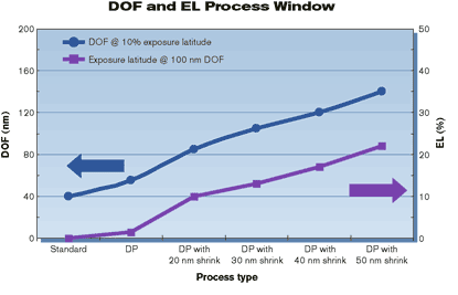
Depth of focus (DOF) and exposure latitude (EL) process window for different amounts of post-lithography CD shrink on a 50 nm contact hole shows that DOF is improved by combining double patterning (DP) with shrink.
Two important metrics for the lithography process window are depth of focus (DOF) and exposure latitude (EL). The Figure shows a DOF and EL window for contact-hole patterning, representative of 32 nm node dense and isolated structures. In this simulation, DOF and EL are modeled for 50 nm final CD contact-hole patterns for various amounts of post-litho CD shrink. As expected, for a 50 nm desired final CD, DP with a large CD shrink can improve the DOF window by up to 350% at a 10% EL. Conversely, an EL of >20% at a 100 nm DOF window can be realized by DP with shrink. Additional capability to tune iso-dense bias during the etch will increase the effective DOF even further.
.
In addition to the in situ deposition capability for CD shrink, the ability to etch in situ multiple film layers is a crucial capability for providing cost-effective DP as these methods are integrated into device manufacturing. Today, in situ etch of full stacks is in production in multiple devices, enabled by etch capabilities such as dynamic wafer temperature control and dynamic gas redistribution, as well as by pre-coat and post-clean techniques to ensure that every wafer sees the same environment.
In summary, critical etches are being added to the overall device process flow through the implementation of DP techniques. Advanced etch technologies used for existing critical etches are adaptable to address the new paradigm in patterning and can deliver performance needed for DP, such as <1.5 nm CD uniformity, pattern shrink and in situ full-stack etching.
Author Information
Raghu Balasubramanian, senior marketing manager for etch businesses at Lam Research, has over 15 years of industry experience in areas ranging from crystal growth, lithography, scatterometry and now etch.
Andy Romano, senior marketing manager for the Patterning Group, spent 10 years working in various fabs, including as a research engineer at the Fairchild Research Center at National Semiconductor, predominantly in photolithography. He was also a global product manager at AZ Electronic Materials for nine years.
Marshall Benham, senior director of product marketing, spent the past 13 years in various technical marketing management roles, predominantly in etch


